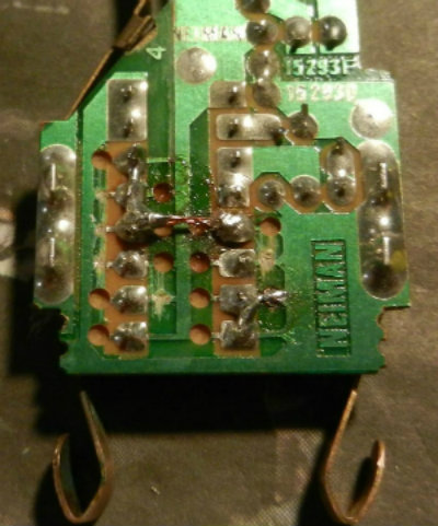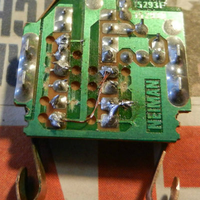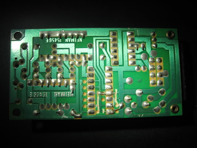
This is a picture of the receiver PCB - If you look underneath the TEA550 chip you can see a row of 6 terminals on the left and 4 on the right which are either connected to the high bus (runs down the centre), the low bus (runs on the outside) or not connected to either. Depending on how these 10 pins are connected determines the 'code' of the the transmitter/receiver combination.
The transmitter has a circuit containing an identical chip, again with inputs connected or not connected, so whatever arrangement you have in the transmitter, you must have the corresponding arrangement in the receiver for it to work. The transmitter circuit has the low bus in the centre, and the high bus on the outside. It's easier to modify the receiver to the transmitter rather than the other way round - more space and it's easier to find a spare receiver should you screw it all up!
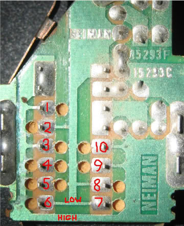
Note that pins 1-10 on the transmitter correspond to 10-1 on the receiver. Also, the logic is reversed so that an input corrected to low on a transmitter should be left unconnected on the receiver and vice-versa. It may help to draw up a table like this:
The H, L, N refer to the pin connections HIGH, LOW, or NOT CONNECTED
Code: Select all
TX pin   LOGIC   LOGIC   RX pin (original configuration in brackets)
   1       H       H        1  (L)
   2       L       N        2  (L)
   3       H       H        3  (H)
   4       N       L        4  (H)
   5       N       L        5  (L)
   6       L       N        6  (H)
   7       L       N        7  (H)
   8       L       N        8  (H)
   9       H       H        9  (H)
10 H H 10 (H)Note how H stays as H, but N becomes L and L becomes N.
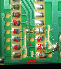
You can see how I've cut the low bus connection to inputs to 1 and 2; and the high bus inputs 4, 6, 7 & 8. That's the easy bit as you can just scribe to cut the tracks.
I've then joined input 1 to the high bus, and input 4 to the low bus using just a single strand of copper wire soldered into place. It's a little bit fiddly but a lot easier than it would be with surface mount components!
EDIT - Thanks for RxBx who spotted the 'deliberate' mistake (got my right and left muddled). Shows that someone was paying attention!


